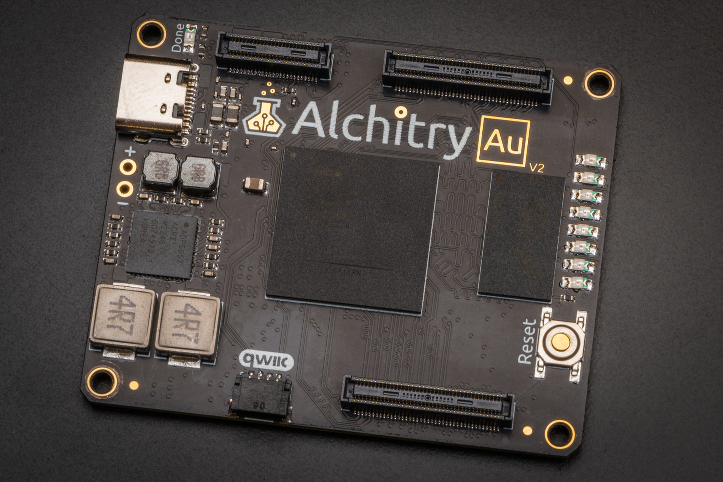
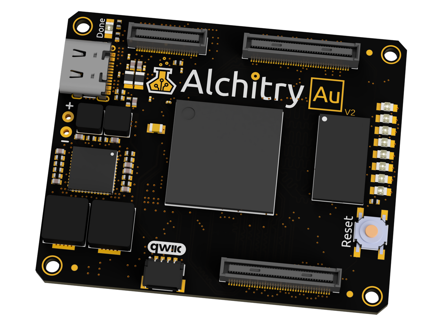
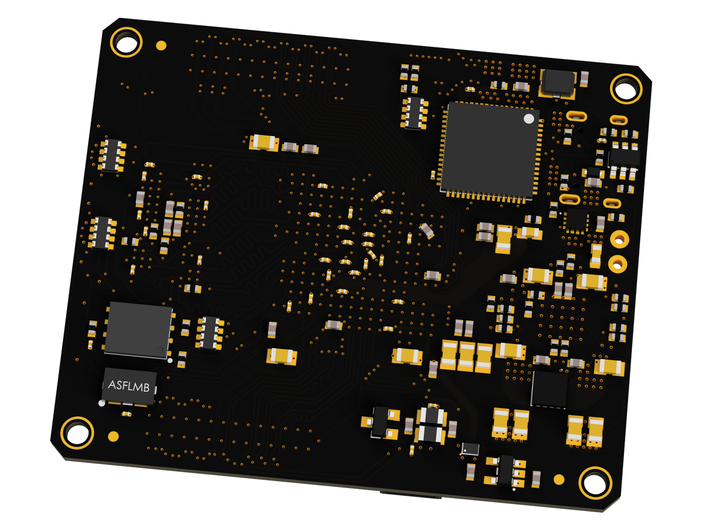
Alchitry Au V2
Alchitry Au V2
Regular price
$114.99 USD
Regular price
Sale price
$114.99 USD
Unit price
per
Couldn't load pickup availability
The Artix 7 FPGA requires a free license for Vivado. Click here for instructions on installing it.
If you're looking for the original Au, click here.
Features
- XC7A35T-2FTG256I FPGA (speed and temperature grade upgrade over Au V1)
- 104 IO pins broken out across two headers
- 20 are triple voltage (3.3V, 2.5V, or 1.8V) of which 18 are LVDS_25 capable
- 44 pins are routed as 100 ohm differential pairs (includes 18 triple voltage pins)
- Remaining IO routed as 50 ohm single ended (~90 ohm when used as diff pairs)
- 2 1.35V pins on bank B
- 8 pairs can be used as inputs to the XADC (0-1V input range)
- Remaining IO is at 3.3V
- All pairs can be used as LVDS_25 inputs except three pairs on bank B
- Control Header
- 8 IO pins also connected to on-board LEDs
- 1 IO pin also connected to on-board reset button
- JTAG
- Analog voltages and dedicated XADC input (0-1V range)
- Raw power input/3.3V regulated output
- QWIIC connector (shares pins on bank B)
- 100MHz oscillator
- 8 general purpose LEDs
- 1 button (typically used as reset)
- 256MB DDR3L @ 800Mb/s (400MHz)
- 32MBit Configuration FLASH
- FT2232HQ USB -> JTAG and USB -> UART (12Mbaud max)
- 5-12V input voltage on-board power supply
- 3.3V @ 4A (IO)
- 2.5V @ 500mA (triple voltage pins, derived from 3.3V)
- 1V @ 4A (VCCINT)
- 1.8V @ 1.2A (VCCAUX, triple voltage pins)
- 1.35V @1.2A (DDR3L)
- 1.8V @ 200mA (analog)
Documents


