Alchitry Pt V2 First Batch
Alchitry Pt V2 First Batch
Couldn't load pickup availability
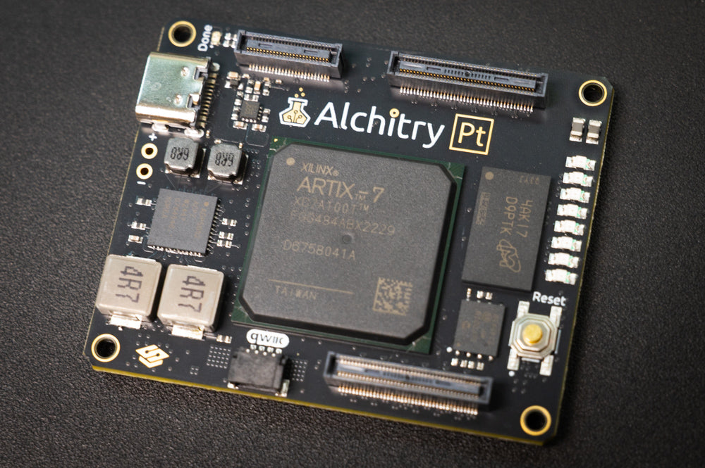
The first batch of Alchitry Pt had some issues...
A few signals on the board weren't connected that should have been and the pinout on bank B was partially scrambled.
This is your chance to snag a killer deal on a Pt from the first batch if you're willing to deal with some of its quirks.
These boards have been reworked so they are fully functioning. The only practical difference between this and the production model is that the pinout is different. Bank B was reworked to put the tri-voltage pins together and a pair from the control header was swapped onto bank B.
Alchitry Labs has the pinout for this model built in so by using the "PT_ALPHA" pinout in your constraints file you can use this like a regular Pt. That is, assuming you aren't using 2.5V or 1.8V with the tri-voltage pins. If you run everything at 3.3V, it is functionally identical.
See the pinout on GitHub for both the top of this board as well as the production pinout. The bottom pinout is the same between models.
The Artix 7 FPGA requires a free license for Vivado. Click here for instructions on installing it.
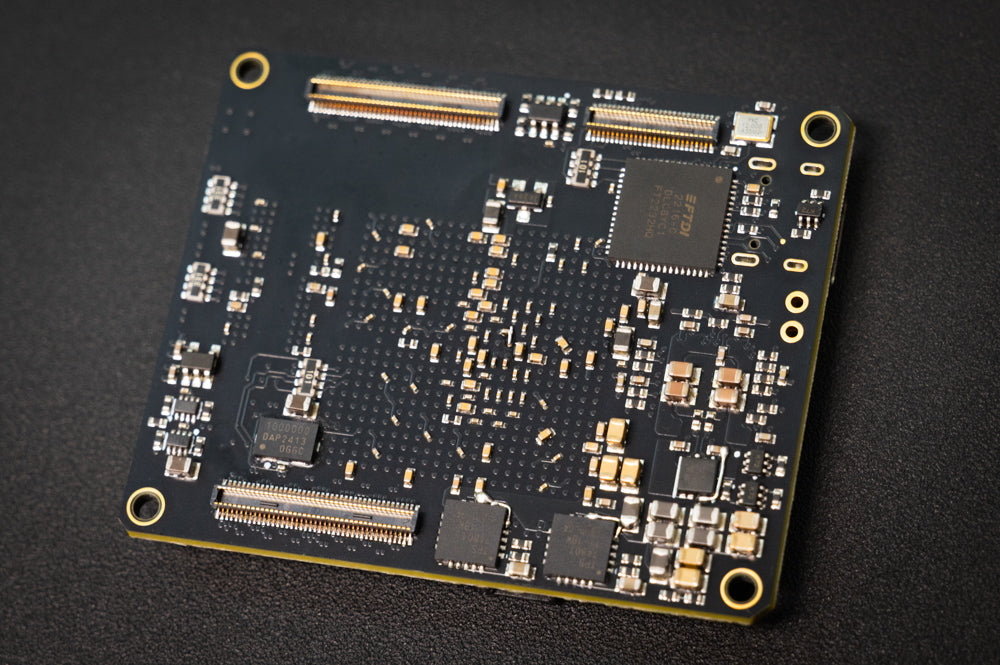
The Pt was designed so that no components on the bottom are taller than 1.5mm allowing a for use of the high speed 1.5mm stack-height DF40 connectors. This requires that the mating board is clear of components under the Pt.
Due to physical conflicts, the bottom side of the Pt cannot be directly connected to the Ft, Ft+, or Hd. A Br, Fn, or Sp must be between the boards to prevent the connectors from contacting capacitors on the bottom the Pt.
Features
- XC7A100T-2FGG84I FPGA
- Connectors on both sides of the board allow two independent stacks (IO isn't shared)
- 206 IO pins
- All IO pairs are LVDS_25 capable inputs or TMDS_33 capable IO
- 112 on the top
- Routed as differential pairs
- 32 triple voltage (3.3V, 2.5V, or 1.8V) pins (16 pairs) capable of LVDS_25 IO
- 8 are on the control header
- 92 on the bottom
- Routed as differential pairs
- 8 are on the control header
- 2 on QWIIC connector
- 20 GTP pins broken out on the bottom
- 2 clock input pairs
- 4 Tx pairs
- 4 Rx pairs
- 6.25 Gb/s bandwidth per pair
- 100MHz oscillator
- 8 general purpose LEDs
- 1 button (typically used as reset)
- 256MB DDR3L @ 800Mb/s (400MHz)
- 32MBit Configuration FLASH
- FT2232HQ USB -> JTAG and USB -> UART (12Mbaud max) or FIFO (~8MB/s)
- 5-12V input voltage on-board power supply
- 3.3V @ 4A (IO)
- 2.5V @ 500mA (triple voltage pins, derived from 3.3V)
- 1V @ 4A (VCCINT)
- 1.8V @ 1.2A (VCCAUX, triple voltage pins)
- 1.35V @1.2A (DDR3L)
- 1.8V @ 200mA (analog)
- 1V @ 1.5A (MGTAVCC, derived from 3.3V)
- 1.2V @1.5A (MGTAVTT, derived from 3.3V)
Documents
Note that the names of signal on bank 16 and bank 34 are swapped in the schematic. This makes no functional difference but may be confusing.